MyScope was developed by Microscopy Australia to provide an online learning environment for those who want to learn about microscopy. The platform provides insights into the fundamental science behind different microscopes, explores what can and cannot be measured by different systems and provides a realistic operating experience on high end microscopes.
Basis
Resolution
\[ d=\frac{0.61\lambda}{nsin\alpha} \]
| Where | Equals |
|---|---|
| \(d\) | resolution (minimum resolvable distance) |
| \(\lambda\) | wavelength of the energy source |
| \(n\) | refractive index of the medium |
| \(\alpha\) | aperture angle |
Note: The term nsinα is named numerical aperture.
Electromagnetic Spectrum

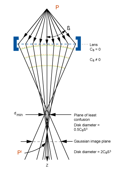
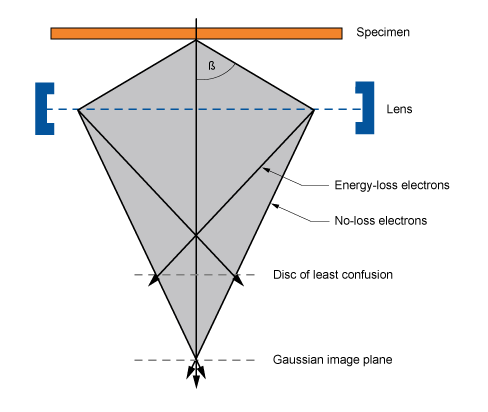
Problems with lenses: aberrations
Microscope Comparisons

| OM | TEM | SEM | |
|---|---|---|---|
| Magnification | 2000x | 5,000,000x | 500,000x |
| Resolution | 200nm | 0.2nm | 20nm |
| Depth of field | 1 unit | 300 unit | |
| Microanalysis | crystal structures, specimen orientations and chemical compositions of phases, precipitates and contaminants through diffraction pattern, X-ray and electron-energy analysis. | chemical composition, crystallographic, magnetic and electrical characteristics |
Microscopy Basics
- Optical
transmitted light
contrasting methods
- phase contrast

dark-field
polarisation
differential interference contrast (DIC)microscopy

The route of light through a DIC microscope. The two light beams should be parallel between condenser and objective
fluorescence
laser microscopy=Confocal microscopy
Digital microscopes
- Electron
transmitted electron microscopy (TEM)
scanning electron microscopy (SEM)
environmental scanning electron (ESEM)
field emision-scanning electron microscopy (FE-SEM)
field emision transmission electron microscopy (FE-TEM)
Micro-probe EM
Energy dispersive spectroscopy EDS (or Energy Dispersive X-ray spectroscopy EDX)
Wavelength Dispersive Spectroscopy (WDS) (or wavelength dispersive X-ray spectroscopy)
SEM-CL:cathodoluminescence
Serial-section Scanning Electron Microscopy
Focused Ion Beam Microscopy (FIB)
Microscopy and Measurement
- Field Number (FN)
- more accurate estimate
- stage micrometers
- ocular reticules
- calibration
Photomicrography
The objective on the microscope is the lens for the camera. This means the aperture is that of the objective. As a result the camera must be set to aperture priority mode.
- Pixels
- Data Processing
- Binning Data
Image Management
- Key Considerations In Modern Digital Systems
- Whether the image is colour or monochrome
- Size of the chip
- Pixel size
- Quantum efficiency
- Readout noise
- Dynamic range in which the image is stored
- Bit depth
- Frame rate at data collection
- Pixel number
- Cooling
- Gain or binning
- Whether the camera is designed for a microscope or consumer use
- Monitor quality
- Reconstruction
- 2D to 3D: Filtered Backprojection
- 3D to Visual Render: voxels (VOlume (X) ELements - similar to a pixel)
Scanning Electron Microscopy
Can & can't
can:
- Image morphology of samples (e.g. view bulk material, coatings, sectioned material).
- Image compositional and some bonding differences through contrast and by using backscattered electrons.
- Image molecular probes by using metal and fluorescent probes in biological samples.
- Undertake micro and nano-lithography (remove material from samples; cut pieces out or remove progressive slices from samples [e.g. using a focussed ion beam]).
- Heat or cool samples while viewing them (this requires a specific type of stage).
- Wet and dry samples while viewing them (only in an Environmental SEM)
- View frozen material using a cryostage
- Analyse X-rays from samples for microanalysis (requires a EDS or WDS detector)
- Study optoelectronic behaviour of semiconductors (requires a cathodoluminescence [CL] detector)
- View/map grain orientation/crystallographic orientation and study related information like heterogeneity and microstrain in flat samples (requires an EBSD detector).
can’t
Image wet samples
Image non-conductive samples
Colour images
Accurate height measurement
Sub-surface imaging
Imaging through fluid
Atomic imaging
Elemental analysis below micrometre scale
Elemental analysis of areas less than 1 micrometre can be very difficult in an SEM. This is due to the interaction volume between the electron beam and the sample which is often in the micrometre range. The interaction volume can be reduced by reducing the electron beam accelerating voltage. However, the corresponding reduction in signal can make it difficult to acquire useful data.
Image charged molecules
Components

Electron gun


Vacuum system
Types of pumps
Rotary pumps
Diffusion pumps
Scroll pumps
Turbo-molecular pumps
Ion getter pumps
Vacuum requirements
- high-vacuum mode: SE mode & secondary electrons
- low-vacuum mode: backscattered electrons & characteristic X-rays
Water chilling system
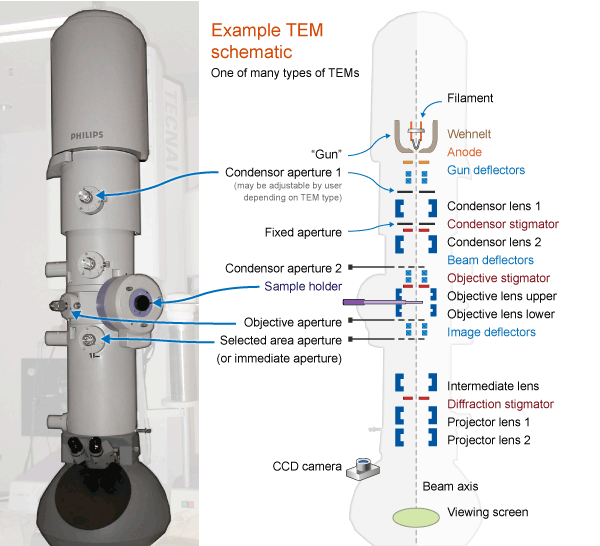
Structure of the column
condenser lens
objective lens
scanning coils (two pairs of electromagnetic deflection coils)
Specimen chamber
- stage
- detectors
Imaging system
- SE images(surface of sample)
- increase the yield of SE <= coat thin layer(~10 nm) heavy metals (gold/platinum)
- non-conductive coated to reduce surface charging
- low atomic number (Z) specimens (e.g. biological samples) coated to provide a surface layer
- increase the yield of SE <= coat thin layer(~10 nm) heavy metals (gold/platinum)
- The contribution of BSE to images collected with the SE detector
- higher kV => sub-surface information due to various backscattered effects (elastic scattering)
- SE1: interaction between primary electron beam and sample
- SE2: generate by BSE
- SE3: interaction of beam with sample chamber, pole piece etc
- higher kV => sub-surface information due to various backscattered effects (elastic scattering)
Beam/specimen interactions

regions
- SE (top 15nm)
- BSE (top 40%)
- X rays (entire region)
Electron-matter interactions
- Elastic scattering: BSE
- Inelastic scattering
- phonon excitation (heating)
- cathodoluminescence (visible light fluorescence)
- continuum radiation (bremsstrahlung)
- characteristic X-ray radiation
- plasmon production (secondary electrons)
- Auger electrons (ejection of outer shell electrons)
Modelling interactions
- Casino (Monte Carlo Simulation of electroN trajectory in sOlids)
A basic guide to using an SEM
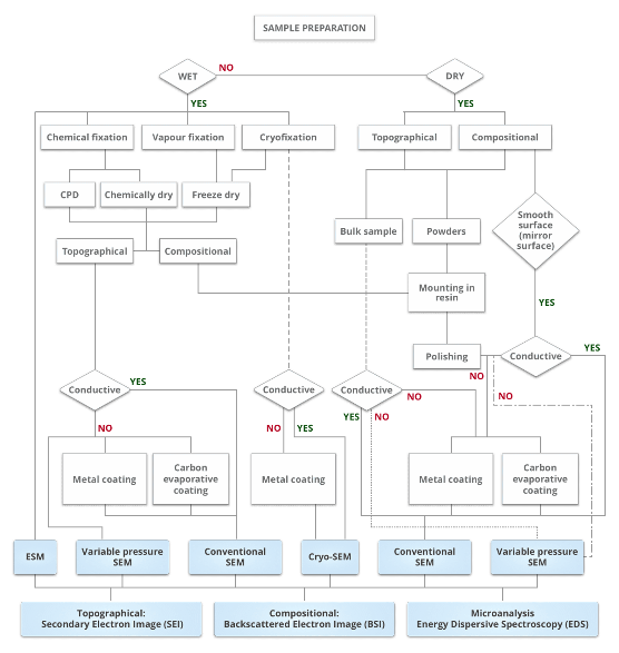
Specimen preparation
Accelerating voltage

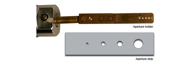
Apertures


Spot size

- working distance smaller => smaller spot size
- condenser lens setting higher current => smaller spot size
- objective lens aperture smaller => smaller spot size
Working distance

Constrast and brightness
- Perfecting an image - Signal processing
- Tilting to increase SE contrast
Magnification & Calibration
Scan rate & signal to noise
- slower scan rate => more electrons at each point => better quality
- quality limited
- spot size
- signal(S)/noise(N)
- Noise <= beam brightness, spot size, SE detector sensitivity => salt-and-pepper, grainy
- high-resolution => low S/N ratio & grainy.
- increase electrons per point => improve S/N ratio
- eg. Tungsten (W) filaments
- high resolution => small spot sizes => low quantity of electrons => low brightness => need high current detecter => low S/N ratio
Image artefacts and trouble-shooting
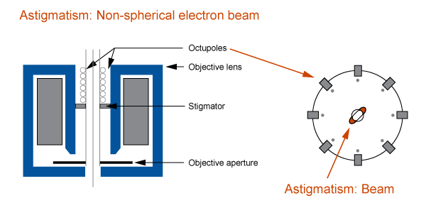
- Astigmatism: stigmator
- Lack of detail of surface structures: lower kVs (5-10kV)
- Edge effects: lower kVs
- Charging
- reduce electron energy(kV)
- reduce number of electrons
- beam current
- emission level of gun
- spot size
- apertures between gun & specimen
- recoat the sample with a thicker layer of platinum
- Specimen damage
- lower beam energy
- increase WD => larger spot size on the sample but reduce resolution
- Beam-related contamination
- take micrographs at low magnification
- ensure sample clean
Specialised SEM techniques
CL
ESEM:
Cryo-SEM-Cold stage
hydrated (wet) samples, delicate biological samples, hydrogels, food, biofilms, foams, fats and waxes, suspensions, pharmaceuticals and nanoparticles
FIB
EDS
EBSD
EBL
Electron beam lithography (EBL) is a maskless lithography technique used for patterning of computer generated layout structures on photoresists on silicon wafers.
Backscatter
electron channelling contrast imaging (ECCI)
The change in diffraction of the backscattered electrons as they interact with a dislocation in the material results in a higher backscattering coefficient than for the matrix; so individual dislocations appear as bright lines in a darker matrix.
Coating
- uncoated for compositional information
- non-conductive coated with carbon with compositional detail
Topography and BSE
- flat => best compositional information
- BSE image (greyscale differences <= atomic number contrast)
- phases recognition & classification
- differences in elemental composition or concentrations
SEM simulator
Transmission Electron Microscopy
Can & can't
can:
- Image morphology of samples, e.g. view sections of material, fine powders suspended on a thin film, small whole organisms such as viruses or bacteria, and frozen solutions.
- Tilt a sample and collect a series of images to construct a 3-dimensional image.
- Analyse the composition and some bonding differences (through contrast and by using spectroscopy techniques: microanalysis and electron energy loss).
- Physically manipulate samples while viewing them, such as indent or compress them to measure mechanical properties (only when holders specialised for these techniques are available).
- View frozen material (in a TEM with a cryostage).
- Generate characteristic X-rays from samples for microanalysis.
- Acquire electron diffraction patterns (using the physics of Bragg Diffraction).
- Perform electron energy loss spectroscopy of the beam passing through a sample to determine sample composition or the bonding states of atoms in the sample.
can't:
- TEM cannot take colour images. Colour is sometimes added artificially to TEM images.
- TEM cannot image through thick samples: the usual sample thickness is around 100-200nm. Electrons cannot readily penetrate sections much thicker than 200nm.
- A standard TEM cannot image surface information.
- The TEM cannot reliably image charged molecules that are mobile in a matrix. For example, some species (e.g. Na+) are volatile under the electron beam because the negative electron beam exerts a force on charged material.
Components
Beam/specimen interactions
Transmission electron microscopy in practice
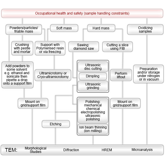
Sample preparation
Organic sample
Inorganic sample
Step-by-step procedures for using TEMs
- Insert the specimen
- Choose and set voltage
- Turn on the gun and filament
- Ensure the illumination system is aligned and operating as needed
- Insert apertures as needed (e.g. objective aperture in if it is out)
- Adjust the sample height to the eucentric position
- Select the correct spot size
- Select the correct aperture size for the apertures needed
- Move the sample to an area of interest and view
- Focus and correct astigmatism
- Select magnification of choice
- Photograph or collect digital recording of image
- Exchange sample or undertake shutdown procedure
Machine settings
| Thin Sections/Biological Samples | High Resolution |
|---|---|
| 80-120 kV | 200-300 kV |
| Condenser aperture: 1 (biggest) | Condenser aperture: 2 or 3 (small) |
| Spot size: 1 (unless sample is “drifting”, 5 or 6) | Spot size: 6 to 8 |
| Objective aperture: 3 (smallest) | Objective aperture: 1 (biggest) |
An increase in voltage
= increased brightness = increased resolution = thicker sections can be used = reduced contrast
The condenser aperture is the top one on the column
A smaller condenser aperture
= increased resolution = decreased beam damage to sample = decreased brightness
The objective aperture is the middle one (just below the specimen holder)
A smaller objective aperture
= increased contrast = decreased brightness
Spot size on the JEM-1010 gets smaller with increasing number
A smaller spot size
= increased resolution (for some imaging modes) = decreased brightness = decreased beam damage to the sample = decreased sample “drift” (stability improved)
Alignment
- Illumination system: beam tilt; beam shift
- Condenser aperture alignment
- Condenser astigmatism correction
- Alignment of illumination with respect to the objective lens
- Objective aperture centering
- Objective astigmatism correction
- Alignment of intermediate lens
Virtual TEM
Additions
Image formation basics
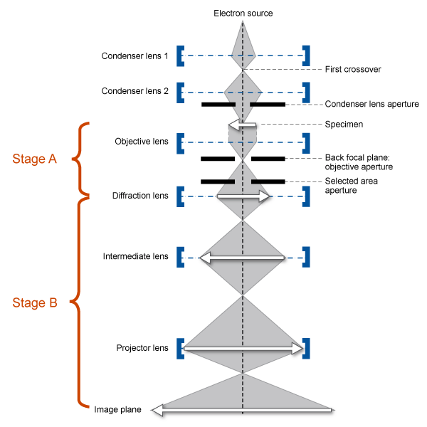
Stage A is the scattering of an incident electron beam by a specimen. This scattered radiation passes through an objective lens, which focuses it to form the primary image.
Stage B uses the primary image obtained in stage A and magnifies this image using additional lenses to form a highly magnified final image.
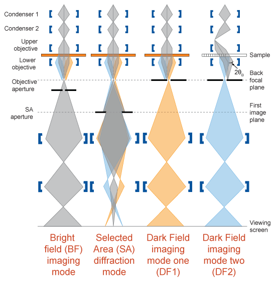
Imaging modes
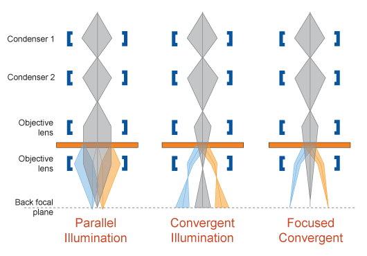
Convergent Beam Electron Diffraction (CBED)
Microanalysis
Energy Dispersive X-ray Spectroscopy (EDS, EDX or XEDS)
| EDS | SEM | TEM |
|---|---|---|
| spatial resolution | 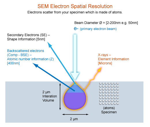 Figure: The typical spatial resolution of different signals, Secondary electrons, Backscattered electrons and X-rays, in the scanning electron microscope. Figure: The typical spatial resolution of different signals, Secondary electrons, Backscattered electrons and X-rays, in the scanning electron microscope. |
order of sample thickness. |
| detection limit | ~0.1-0.5 wt% | ~0.01-0.1 wt% |
X-rays Generation
Bremsstrahlung X-rays
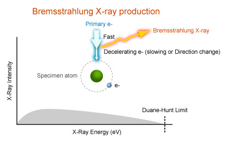
Kramer's law
\[ I=i_p\cdot Z\frac{E_0-E}{E} \]
\(i_p\)(electron probe current),\(Z\)(mean atomic number),\(E_0\)(energy of the electrons in the primary beam)
Characteristic X-rays
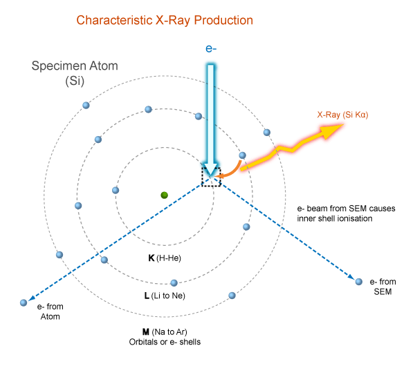
Nomenclature
- Siegbahn: element name + electron shell produce the X-ray + relative intensity of the line
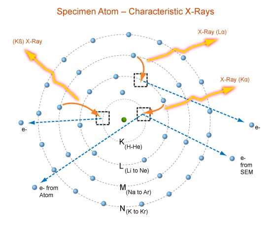
- IUPAC
The X-ray spectrum
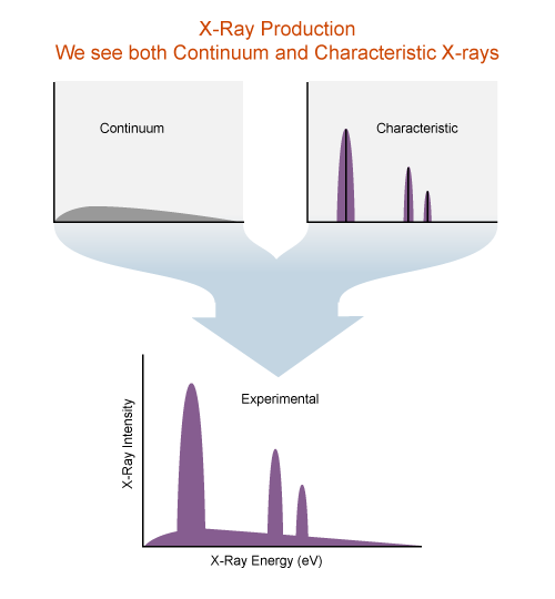
X-ray intensity
Concentration
- major elements (> 10 wt%)
- minor elements (1-10 wt%)
- trace elements (<1 wt%)
Beam current, probe current or spot size
Accelerating voltage or overvoltage ratio
\(\text{overvoltage ratio }U=\frac{\text{electrons energy of primary beam }E_0}{\text{critical ionization energy }E_c}\)
\(U\ge2\) & \(U_{opt}\sim2.7\)
Fluorescence Yield
\(\text{fluorescence yield}=\frac{\text{X-rays}}{\text{Auger electrons}}\)
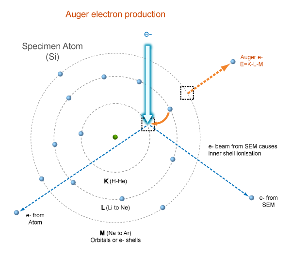
Figure: After inner shell ionization, the atom may relax by emitting a Characteristic X-ray or an Auger electron. The energy of the Auger electron is related to the electronic configuration of the atom that was ionized by the primary electron beam. X-ray Absorption
photo-electric effect
X-ray detection by EDS
Three basic parts
detector (SDD=silicon-drift detector)
pulse processor
Process time, dead time
multi-channel analyser or computer display